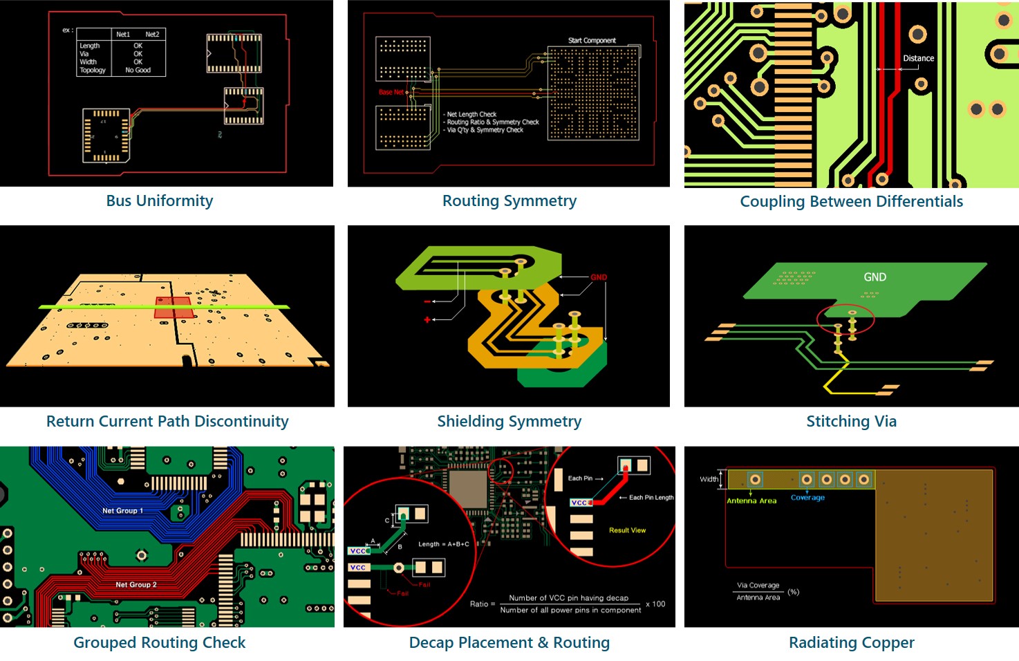
Within memory subsystems major examples include double-data-rate DDR SRAM DDR synchronous DRAM SDRAM synchronous-graphics RAM and Direct Rambus DRAM. In addition to compliance testing Rohde and Schwarz DDR test solutions help you efficiently verify and debug your design at the board and system level.

Figure 2 From Asic Implementation Of High Speed Pipelined Ddr Sdram Controller Semantic Scholar
The end result is a high-bandwidth high-density low-energy memory system thats unlike anything on the market today.

. The Real Difference is in the Cube. SDRAM is a CMOS high-speed dynamic random access memory DRAM and it is configured as a quad-bank Dynamic RAM internally with a synchronous interface means that all signals are registered on the falling or rising edge of the clock signal CLK. The transmitters are designed using 45-nm CMOS process.
Microns Newest Memory Innovation Weve combined fast logic process technology and advanced DRAM design to create an entirely new category were calling Hybrid Memory Cube HMCtechnology. Figure 4- FPGA As Memory Controller. 3 DDR Interface Design Implementation A Lattice Semiconductor White Paper Where DRAM Gets Used 43B Units PC 48 Other Servers 3 14 Peripherals 4 Consumer 10 Graphics 9 Comm 12 Figure 1 Market analyses indicate that DDR is currently utilized in over 50 of all electronic systems and usage is expected to increase to 80 over the next.
Readwrite access to the SDRAM are burst type. High speed DDR memory interface design Abstract. Additionally students will learn about the tools available for high-speed memory interface design debug and implementation of high-speed memory interfaces.
This work presents two high-speed transmitter designs for 24 Gbps Double Data Rate Generation 3 DDR3 memory interfaces. Labs are available for DDR3 on the Kintex-7 FPGA KC705 board. Because numerous memory topologies and interface frequencies are possible on the DDR interface Freescale highly recommends that the board designer verify through simulation all aspects signal integrity electrical timings and so on before PCB fabrication.
Additionally students will learn about the tools available for high-speed memory interface design debug and implementation of high-speed memory interfaces. Any AC timing parameters within this document are for reference. The major feature of DDR interface compared to a single data rate SDR one is to use both rising and falling edges of a clock to transfer data which allow it to.
Learning about the tools available for h. The major feature of DDR interface compared to a single data rate SDR one is to use both rising and falling edges of a clock to transfer data which allow it to provide two times the throughput at the same clock frequency. The design engineer can no longer simply connect data and address lines and expect to have a robust high-speed memory interface.
Summary form only given. The emphasis is on. Accesses start at a selected location selected by.
Ddr Memory And Interface Design Trends Keywords. They are designed for high-performance. Preparing to Simulate DDR Memory Bus Interfaces Published.
Ddr Memory And Interface Design Trends Author. The major memory types covered are DDR2 and DDR3. As part of the overall design DDR memory controller and memory devices also need to properly work in the presence of other high-speed interfaces or even wireless signals.
Moreover output slew rate of both transmitters is controlled at 46 Vns while their output impedance can be programmed between 20 30 and 40 Ω respectively. All the major challenges discussed in this paper have to be overcome for excellent signal integrity to guarantee minimum bit error rate in the multi-Gigabit transmission. These in fact are not the separate issues as they are often viewed to be.
RLDRAMII LPDDR2 and QDRII. Course Description This course teaches hardware designers who are new to high-speed memory IO to design a memory interface in Xilinx FPGAs. The newest members of the Fast Cycle RAM FCRAM series are 256 Mbit high-speed memories that incorporate the double data rate DDR SDRAM interface.
The second of a series on DDR considers how to speed up the process of designing a functioning system. It introduces designers to the basic concepts of high-speed memory IO design implementation and debugging using 7 series FPGAs. The major feature of DDR interface compared to a single data rate SDR one is to use both rising and falling edges of a clock to transfer data which allow it to provide two times the throughput at the same clock frequencyThe high speed up to 16 GHz for DDR III nature and complex timing issues take the most attention for designers of ASIC chips with DDR memory controllers.
DDR4 SDRAM operates at high data rate ie from 16Gbps to 32Gbps and the memory interface must be designed in a stringent way to comply with the specification set by JEDEC. The major memory types covered are DDR2 and DDR3. The high speed up to6 GHz for DDR III nature and complex timing issues take the most attention for designers of ASIC chips with DDR memory controllers.
The major feature of DDR interface compared to a single data rate SDR one is to use both rising and falling edges of a clock to transfer data which allow it to provide two times the throughput at the same clock frequencyThe high speed up to 16 GHz for DDR III nature and complex timing issues take the most attention for designers of ASIC chips with DDR memory. The non-ideal PDN invariably affects some of the most common SI analysis parameters including. The major feature of ddr interface compared to a single data rate sdr one is to use both rising and falling edges of a clock to transfer data which allow it.
Ddr memory and interface design trends Created Date. As the bandwidth requirement increases Double Data Rate DDR interface is becoming very commonly used in many types of memories such as DDR IIIIII DRAM RLDRAM III QDR IIIII SRAM etc. Also be sure to consult the latest errata.
Value of DDR Memories from Market Eye Good Balance of High DensityLow Cost and Small PackageHigh SpeedLow Power Flash offers high density and nonvolatility but very slow write speeds SRAM offers low standby power high-speed operation and requires no refresh but costs increase due to large die sizes. As the bandwidth requirement increases Double Data Rate DDR interface is becoming very commonly used in many types of memories such as DDR IIIIII DRAM RLDRAM III QDR IIIII SRAM etc. In the previous article 1 we discussed some critical signal integrity concerns engineers face while designing the DDR bus.
Introducing the basic concepts of high-speed memory IO design implementation and debug using Xilinx 7 series FPGAs. The major feature of DDR interface compared to a single data rate SDR one is to use both rising and. The following memory types are covered on demand.
However there is a wider scope to consider for accurately perceiving the effects of the IO data signals SI analysis and the power and ground planes PI analysis in high-speed DDR memory interfaces. In the previous article 1 we discussed some critical signal integrity concerns engineers face while designing the DDR bus. Further complicating the implementation of a DDR design is the need to handle and pre-process strobe signals as opposed to generic clock signals.
01 July 2016 The second of a series on DDR considers how to speed up the process of designing a functioning system. Given these challenges it is usually wise to simulate the design before fabricating the board.

Pin On Signal Integrity Analysis
Double Data Rate Ddrx Memory What Is It And How Do You Improve Its Design

Oem Ddr3 1600mhz 204 Pin High Speed Ram Computer Memory Ddr Price In 2022 Ram Computer Computer Memory Ram Memory
Pdf High Performance Axi Protocol Based Improved Ddr 3 Memory Controller With Improved Memory Bandwidth Semantic Scholar
Xilinx Ltd Goodbye Ddr Hello Serial Memory

Ddr Controller Ip For Soc Designs Cadence Ip

Edge Tech 2gb Ddr3 Sdram Memory Module 2gb 2 X 1gb 1333mhz Ddr3 1333 Pc3 10600 Non Ecc Ddr3 Sdram 240 Pin Memory Module Funny Phone Cases Memories
Ddr 4 3 Memory Controller Ip 2400mhz
0 comments
Post a Comment